1) The interval between application of an input step function & the time when the output crosses the value of logic threshold voltage of comparator is nothing but ______.
a. Strobe Release Time
b. Response Time
c. Settling Time
d. None of the above
|
Answer
Explanation
|
ANSWER: Response Time
Explanation:
Typical electrical parameters of comparator include positive & negative output levels, strobe current & strobe release time, response time & saturation voltage. Thus, the interval between input step function & the duration of crossing logic threshold voltage at the output gives the conceptual idea of response time. On the other hand, the time required for rising the logic threshold voltage at the output after the driving session of strobe terminal is conducted from zero to one logic level. Eventually, the parameter of settling time is totally not involved in comparators.
|
|
2) Which among the following parameters is usually only specified in dual and quad level Op-amps which is precisely known as amplifier to amplifier coupling?
a. Average Temperature coefficient
b. Channel Separation
c. Gain-Bandwidth Product
d. Offset V & I Stability
|
Answer
Explanation
|
ANSWER: Channel Separation
Explanation:
Channel separation is a measure of the amount of electrical coupling between the op-amps which are integrated on a semantic chip. This parameter is specifically highlighted in datasheet specifications of dual & quad Op-amps like μAF772 & μAF774 respectively.
Whenever there is an application of signal to input of only one op-amp, then some of the other signal appears on the output confined level of other op-amps due to physical vicinity of op-amps in dual and quad form of packages.
However, the amplitudes of all these signal are almost similar and therefore, can be evaluated with an assistance of channel separation. This conceptual characteristic of parameter specification & mechanism is supposed to be referred as 'amplifier to amplifier coupling'.
|
|
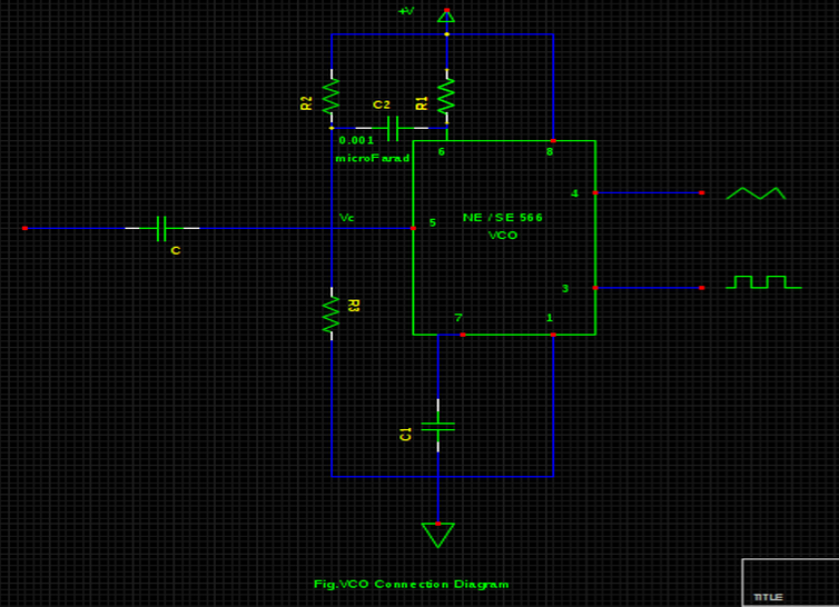
3) For the circuit shown below, +V = 15V, R2 = 1K, R1 = R3 = 8K & C1 = 0.001μF. Compute
(a) nominal frequency of output waveforms &
(b) Modulation in the output frequencies if Vc changes in the mist of 10V to 11.5V.
 a.
a. 26.17 & 33.34 kHz
b. 35.60 kHz & 10 kHz
c. 30.47 kHz & 10 kHz
d. 22.56 & 33.34 kHz
|
Answer
Explanation
|
ANSWER: 30.47 kHz & 10 kHz
Explanation:
(a) By applying voltage -divider rule, initial voltage at terminal 5 is given by,
Vc = (20K) (15) / 11.5K = 26.09 V
Thus, the frequency of output waveform (nominal frequency) is approximated by,
fo ≈ 2(+V - Vc) / R1C1 (+V)
= 2 (15 – 10.43) / (20K x 10-9) x (15)
= 30.47 kHz
(b) Thus, the modulation in the output frequencies can be calculated by initially substituting Vc = 10V & then 11.5 V
fo = 2 (15 – 10) / 20K x 10-9 x 15
= 33.34 kHz
fo = 2 (15 – 11.5) / 20K x 10-9 x 15
= 23.34 kHz
Hence, the variation in an output frequency can be evaluated by the difference between these both frequencies.
i.e. 33.34 - 23.34 = 10 kHz.
|
|
4) Determine the values of load current and output voltage respectively for the below schematic of voltage to current converter with grounded load by assuming that the op-amp is nulled at the inception.
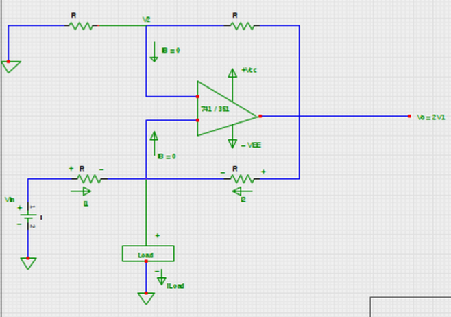 a.
a. 0.3 mA & 4V
b. 30 mA & 4V
c. 300 mA & 2V
d. 30 mA & 2V
|
Answer
Explanation
|
ANSWER: 0.3 mA & 4V
Explanation:
Given data :
From the circuit, the given values are:
Vin = 10V, R = 30K & V1 = 2V
We know that load current depends on input voltage resistance R in case of voltage to current converter.
Thus, IL = Vin / R
= 10V / 30K
= 0.3 mA
However, the output voltage (Vo) of voltage to current converter is given by,
Vo = 2 V1 = 2 x 2 = 4V.
|
|
5) What will be the values of bandwidth & maximum output voltage swing respectively in an non-inverting amplifier with input resistance of about 40 ohm, input capacitance of about 0.1μF with inclusive of R1=R2=R3=200K Ω, Rf = 2M Ω and Vcc = + 20V?
 a.
a. 32.56 kHz & 20 Vpp
b. 30.56 kHz & 20 Vpp
c. 47.56 kHz & 20 Vpp
d. 67.56 kHz & 20 Vpp
|
Answer
Explanation
|
ANSWER: 47.56 kHz & 20 Vpp
Explanation:
In accordance to given data, the ac input resistance of the amplifier can be given by,
Rif = (R2)¦(R3)¦ [Ri (1+AB)]
When [Ri (1+AB)] >> R2 or R3 then, the above equation becomes
Rif ≈ (R2)¦(R3)
≈ 200K ¦ 200K
= 100K Ω
The low frequency cut-off limit can be exaggerated using
fL = 1 / [2 πCi(RiF + R0)]
= 1 / [2 π (0.1 x 10 -6) (100K +40 )]
= 62.8 Hz
The gain of an amplifier is = 1 + (Rf / R1)
= 1 + (2M / 100K)
= 21
From the formula of Unity gain bandwidth,
UGB = Af x FH
Therefore, fH = UGB / Af = 1 M / 21 = 47.61 Khz
Bandwidth = FH – FL = 47.61 Khz – 0.0476 KHz = 47.56 KHz &
Ideal Maximum Output Voltage Swing = +Vcc = +20Vpp.
|
|
6) What will be the output of differentiator circuit if input sinusoidal voltage has a peak value of 7mV & frequency of 1KHz when the values of resistance and capacitors are R = 1500K and C = 2μF respectively?
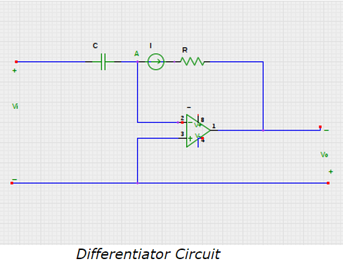 a.
a. -1000 π cos 2000 πt
b. -2000 π cos 2000 πt
c. -42000 π cos 2000 πt
d. -21000 πcos 2000 πt
|
Answer
Explanation
|
ANSWER: -42000 π cos 2000 πt
Explanation:
Given data:
Voltage Peak Value = 7mV
Frequency = f = 1KHz
R = 1500K Ω
C = 2μF = 2 x 10⁻⁶ F
An input voltage equation of a differentiator circuit can be expressed by,
V1 = Asin2 πft
= 7 sin2π x 1000 t
= 7 sin2000π t mV
Scale Factor = -CR = - [2 x 10-6 x 15 x 105]
= - [30 x 10-1 ]
= -3
Hence, the output voltage of differentiator circuit can be evaluated as:
Vo = -3 d / dt [7 sin 2000 π t]
= -3 x 7 x 2000 cos 2000 π t
= -42000 π cos 2000 π t mV.
|
|
7) What will be the designing components for designing second order low pass filter at a high cut-off frequency of 1kHz assuming C = 0.0047μ F along with consideration of standard pot values?
a. R2, R3 = 33k Ω, C1 = C2 = 0.0047μ F, R1 = 27k Ω & Rf = 15.8k Ω
b. R2 = R3 = 66k Ω, C1 = C2 = 0.0047μ F, R1 = 35k Ω & Rf = 60k Ω
c. R2 = R3 = 51k Ω, C1 = C2 = 0.0047μ F, R1 = 67k Ω & Rf = 70k Ω
d. None of the above
|
Answer
Explanation
|
ANSWER: R2, R3 = 33k Ω, C1 = C2 = 0.0047μ F, R1 = 27k Ω & Rf = 15.8k Ω
Explanation:
Since the value of high cut- off frequency is mentioned. Below enlisted are the steps to evaluate filter components of second order low pass filter for designing purpose.
Step 1 : Assume R2 = R3 = R & C1 = C2 = C.
Step 2 : Select the value of C = 1μ F
Suppose that C1 = C2 = C = 0.0047μ F
Step 3 : Determine R by using formula R = 1 / 2 π fH C
R2 = R3 = 1 / (2 π x 103 x 47 x 10-10)
= 33.86k Ω
(consider the round figure value i.e. 33k Ω
As we know that Rf should be equal to 0.586 x R1, then R1 = 27k Ω)
Thus, Rf = 0.586 x 27 = 15.86k Ω
By taking into consideration the pot value of about 20k Ω, estimated resistances are
R2 = R3 = 33k Ω
C2 = C3 = 0.0047μ F
R1 = 27k Ω & Rf = 15.8k Ω
Step 4 : Since the values of resistors and capacitors are equal , the passband voltage gain must be equal to Af = 1 + (Rf / R1) 1.586
However, the gain must satisfy the Butterworth response & hence, the value of R1 must be selected = 100k Ω in order to estimate the value of Rf.
|
|
8) The below drawn schematic of Op-amp 741 is configured in non-inverting mode with R1 = 2 K Ω, Rf = 20 K Ω, fo = 10 Hz & A = 4,00,000. Determine the following parameters :
1) Af
2) fF
 a.
a. 10.99 & 90.9 kHz
b. 10.99 & 36.36 kHz
c. 10.99 & 20 kHz
d. 10.99 & 10 kHz
|
Answer
Explanation
|
ANSWER: 10.99 & 36.36 kHz
Explanation:
For non-inverting mode of an amplifier (voltage series feedback amplifier)
1) Af = AB / 1 + AB
But, B = R1 / (R1 + Rf) = 2 k / (2 k + 20 k)
= 1 / 11
1 + AB = 1 + 400000 x (1 / 11)
= 36364.6
Af = 400000 / 3636.4 = 10.99
2) fF = (1 + AB) fo = (36364.6) x 10Hz = 363646 = 36.36 KHz
|
|
9) Which transistor array is essential in construction of a mirror circuit where the formation of diode takes place by an adjacent transistor?
a. CA3081
b. CA3046
c. CA3086
d. CA3083
|
Answer
Explanation
|
ANSWER: CA3086
Explanation:
CA3086 play a significant role in proper execution or operation of the circuit during the construction of mirror circuit. Here, the diode gets formed with an assistance of transistors placed adjacently. However, this type of transistor array ultimately leads to acquire the thermal stability and the requisite amount of collector current in a current mirror circuit.
Due to simplicity in fabrication and operation, current mirror circuit have wide range of applications in the aspects of differential and operational amplifiers.
|
|
10) What is the connection configuration of swamping resistor in case of a differential amplifier?
a. In series with each emitter
b. In series with each collector
c. In parallel with each collector
d. In parallel with each emitter
|
Answer
Explanation
|
ANSWER: In series with each emitter
Explanation:
External resistor of a differential amplifier is connected in series combination with each emitter. Due to this configuration, the dependability of voltage gain which varies in accordance to changes in emitter resistance can be ablated. Apart from this advantage, external resistor also possesses a beneficiary notion of increasing the linearity range of differential amplifiers.
However, the value of external resistor has an efficiently high value to swamp the consequences of emitter resistor of amplifier. As a result, this external resistor is also renowned as 'Swamping Resistor' because of its swamping strategy.
|
|


